Overview
Turning a circuit concept into a manufacturable board
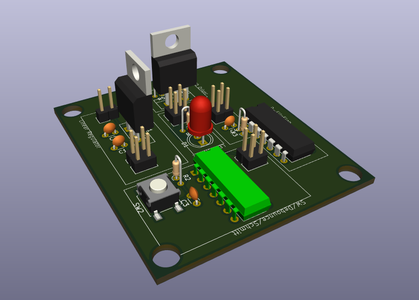
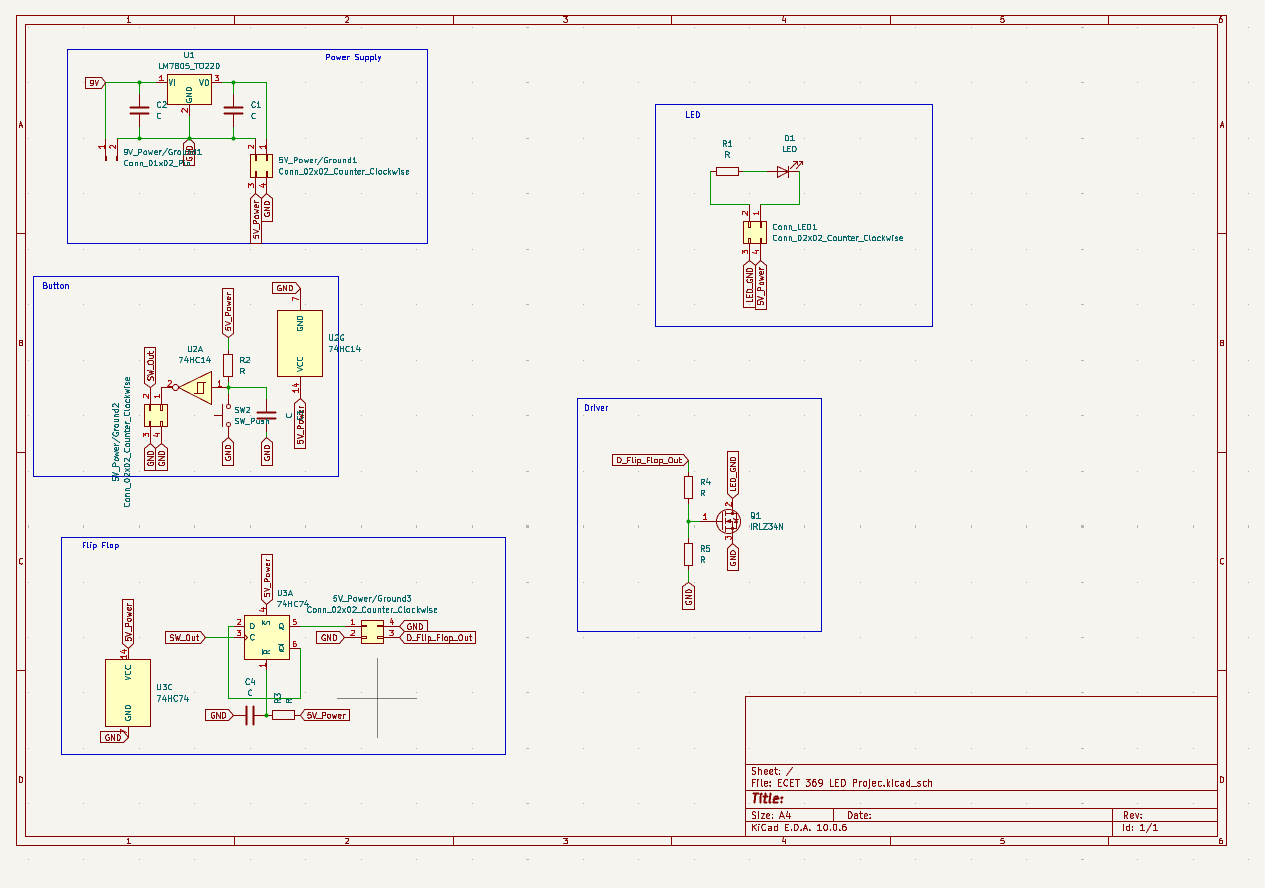
This board was developed for a group project in a junior-year computer vision course. A 9 V battery feeds a linear regulator that produces the 5 V rail used by the logic circuit. Pressing the momentary button sends a conditioned signal through a Schmitt trigger to reduce the effects of contact bounce. A D-type flip-flop stores the toggle state, and its output controls a MOSFET that completes the LED's path to ground. My responsibility was to translate the team's circuit requirements into the complete schematic and physical PCB design.
The challenge
One button press needed to produce one reliable state change.
A mechanical pushbutton does not create a perfectly clean transition; contact bounce can generate several rapid edges from a single press. That behavior could clock the flip-flop multiple times and make the LED state unpredictable. The circuit also needed compatible voltage levels across the 9 V input, 5 V logic rail, digital components, and MOSFET-driven LED stage while remaining practical to breadboard and manufacture.
Responsibilities
From initial sketch to fabrication-ready PCB
Sketch the architecture
Started with pen and paper to define the power, button-conditioning, state-storage, and LED-driver blocks before entering the circuit in CAD.
Research components
Reviewed component specifications and pinouts to confirm that the regulator, Schmitt trigger, flip-flop, MOSFET, and LED stage could operate together at the intended voltage and current levels.
Breadboard and verify
Built the circuit on a breadboard to test the initial schematic and confirm the expected toggle behavior before committing to a PCB layout.
Design and order
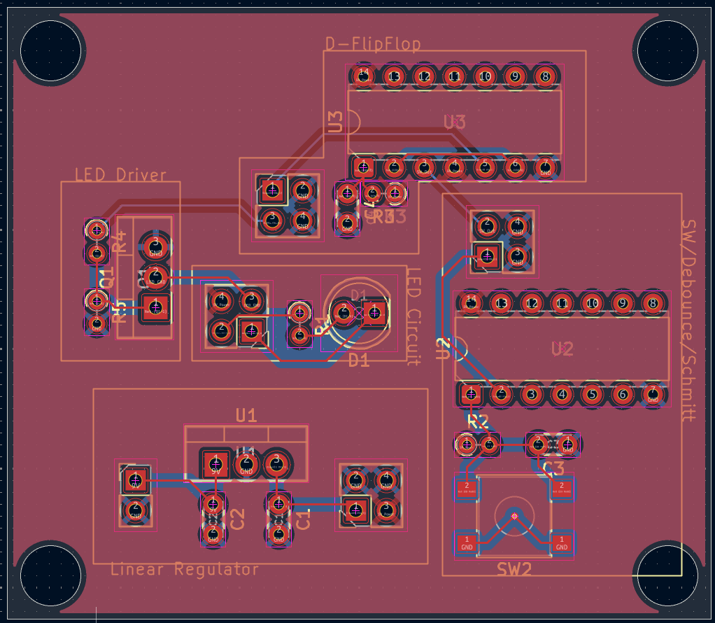
Created the KiCad schematic, assigned footprints, placed components by functional block, routed the board, reviewed the 3D model, and prepared the design for fabrication.
Final architecture
Regulate. Condition. Latch. Drive.
The final design separates the system into four functional stages: a 5 V regulated power supply, Schmitt-trigger input conditioning, D flip-flop state storage, and a MOSFET low-side LED driver. Organizing the schematic and PCB around these blocks made the signal path easier to validate, route, review, and troubleshoot before the board was ordered.
Scope